What do 3nm and 2nm actually mean? The chip number that stopped being a size
Measure every part of a 3nm chip and nothing on it comes out at 3 nanometers. The number names a generation, much like a car model number.
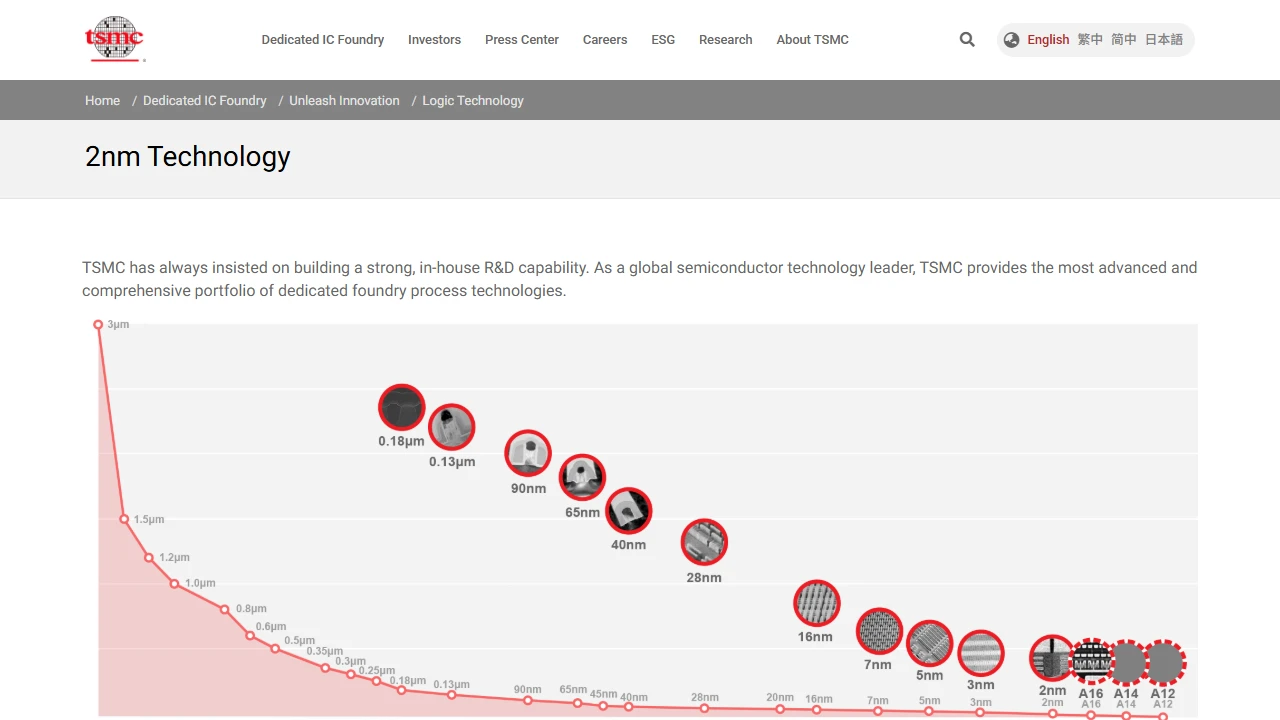
3nm and 2nm are not the length of anything on a chip. At the IEDM conference in December 2022, TSMC disclosed one real dimension of its N3 process: the distance between the centers of neighboring transistor gates is 45 nanometers, fifteen times the name. The name and the geometry went separate ways long ago. Today a nanometer figure tells you which generation a process belongs to, and nothing about how long any part of it is.
- What engineers actually measure
- When the name and the size parted ways
- Samsung, TSMC and Intel mean different things by 3nm
- The transistor has changed shape twice
- Reading a claim like 23% faster or 45% less power
- How much the number should count when you buy
- After 2nm, the names switch to angstroms
- FAQ
What engineers actually measure
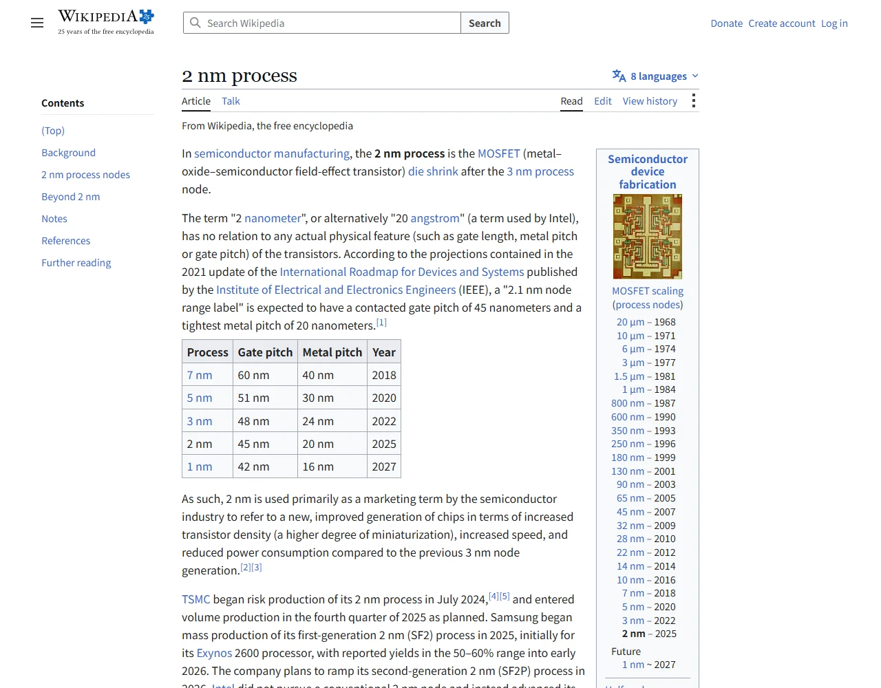
A logic chip is a dense grid of transistors, and each transistor has a gate that works like a valve, letting current through or shutting it off. When engineers want to know how tightly a process packs things, two numbers come up most. One is the gate pitch, the distance between the centers of two neighboring gates, which sets how closely a row of transistors can sit. The other is the minimum metal pitch. Layer upon layer of metal wiring sits above the transistors, and the tightest spacing between two wires in the bottom layer decides how densely the connections can be routed.
The International Roadmap for Devices and Systems (IRDS), published under the IEEE, attached projected dimensions to each node name in its 2021 edition. Line them up and the gap between name and geometry is plain:
| Name | Gate pitch | Minimum metal pitch | Roadmap year |
|---|---|---|---|
| 7 nm | 60 nm | 40 nm | 2018 |
| 5 nm | 51 nm | 30 nm | 2020 |
| 3 nm | 48 nm | 24 nm | 2022 |
| 2 nm | 45 nm | 20 nm | 2025 |
| 1 nm | 42 nm | 16 nm | 2027 |
From 7 to 2, the name shrinks by more than three times, while the gate pitch only goes from 60 to 45 nanometers, a quarter less. Even the roadmap's 1 nm still has a 42-nanometer gate pitch. These are roadmap projections and each manufacturer's real figures differ; the N3 gate pitch TSMC disclosed is 45 nanometers, a little tighter than the 48 in the table.
So what does a new generation actually improve? Mostly density. Pitches shrink a little, transistor structures and layout tricks add more, and the same area holds noticeably more transistors. When a foundry says faster or more efficient, most of it traces back to that extra density.
When the name and the size parted ways
They used to be the same thing. When a process was called 3 micrometers or 1 micrometer in the 1970s and 1980s, that was the length of the transistor gate, something you could measure under a microscope. Wikipedia's article on semiconductor device fabrication puts it bluntly: the number stopped matching gate length around 1994, and since 2009 the node has been a commercial name for a new generation of process technology, with no relation to gate length, metal pitch or gate pitch.
Why did the numbers keep falling? The industry ran on a rhythm for decades. Shrink each linear dimension to about 70 percent of the previous generation and the area roughly halves, so the same chip holds twice as many transistors. Node names followed roughly the same ratio: 22, 14, 10, 7, 5, 3, 2. When plain shrinking got hard, manufacturers chased the halved area with 3D structures and other tricks, and the names kept marching down on the old schedule.
Philip Wong, who heads corporate research at TSMC as a vice president, offered an analogy at the Hot Chips conference in 2019: the numbers are like car models, a BMW 5 Series or a Mazda 6. They name the next technology, and the number itself does not matter.
Samsung, TSMC and Intel mean different things by 3nm
Because each company names its own processes, the same number can mean quite different things. In 2022 Samsung and TSMC both announced 3nm production, and they did not even build the same kind of transistor.
Samsung announced at the end of June 2022 that it had started 3nm production, and it jumped straight to a gate-all-around (GAA) transistor, which it calls MBCFET. At a shipment ceremony that July, the first batch went to a Chinese company that designs cryptocurrency mining chips. Samsung compared the process with a 5nm process it did not name: 16 percent higher transistor density, and either 23 percent more performance or 45 percent lower power.
TSMC announced on December 29, 2022 that N3 was in volume production, still using FinFET transistors; its own site calls N3 a 3nm FinFET technology. It saved gate-all-around for the next generation. According to TSMC, N2 uses its first generation of nanosheet transistors and entered volume production in the fourth quarter of 2025.
Intel shows best how loose the names are. In July 2021 it renamed its processes outright: what had been 10nm Enhanced SuperFin became Intel 7, the next ones Intel 4 and Intel 3, and after those came 20A and 18A, counted in angstroms. Wikipedia's fabrication article offers a useful comparison: TSMC's and Samsung's 7nm are defined much like Intel's 10nm. In September 2024 Intel dropped 20A to focus on 18A, and Panther Lake, unveiled in October 2025, is its first processor platform built on 18A.
Even the IRDS wrote in its 2021 edition that there is not yet a consensus on node naming across foundries and chipmakers. Here is how the labels you see at launch events and on spec sheets line up:
| Label on the spec sheet | Whose | Transistor | Public milestone |
|---|---|---|---|
| N3, N3E, N3P (often written as 3nm) | TSMC | FinFET | N3 volume production announced December 2022 |
| 3GAA (3nm) | Samsung | GAA (MBCFET) | Start of production announced end of June 2022 |
| N2 (2nm) | TSMC | Nanosheet (GAA) | Volume production from Q4 2025 |
| Intel 7 | Intel | FinFET | Formerly 10nm Enhanced SuperFin, renamed July 2021 |
| 18A | Intel | RibbonFET (GAA) plus PowerVia backside power | First product, Panther Lake, unveiled October 2025 |
| A16 | TSMC | Nanosheet plus backside power rail | After 2nm on TSMC's roadmap, marked at 2026 |
The transistor has changed shape twice
The names can be arbitrary, but the structural changes are real. Think of a transistor as a soft hose and the gate as a hand squeezing it. The firmer the grip, the more completely it shuts off and the faster it opens. As transistors shrink, failing to shut off becomes the big problem: current leaks past a closed valve and turns into wasted heat.
In the old planar transistor, the hand could press the hose from one side only, the top. Intel was the first to put FinFETs into mass-produced chips, at 22nm, with Ivy Bridge in 2012: the channel stands up like a fin and the gate wraps it on three sides, which brought leakage back under control. For the next decade everyone's 14, 10, 7 and 5nm processes, and TSMC's 3nm too, were built on fins.
Fins ran out of room as well. An industry analysis cited by Wikipedia described TSMC's 3nm as an incremental step, because fin height, gate length and the number of fins per transistor had all hit their limits. The next step is gate-all-around: slice the channel into a few flat sheets stacked on top of each other and let the gate surround every sheet on all four sides. Samsung at 3nm, TSMC at 2nm and Intel at 18A all moved to this family, each under its own name: MBCFET, nanosheet, RibbonFET.
The changes after that go beyond the transistor. One is backside power. Power and signal wires used to share the same stack of metal layers on the front of the chip; now the power lines move to the back of the wafer and the front is left to signals. Intel's PowerVia in 18A and TSMC's backside power rail in A16 follow this idea. Another is stacking the two kinds of transistor on top of each other. Intel, Samsung and TSMC have all shown stacked transistors at research conferences, and production is still some way off.
Reading a claim like 23% faster or 45% less power
Every new process arrives with a set of percentages. Put a few public ones side by side and the reading rules become clear:
| The claim | Compared with | The word to watch |
|---|---|---|
| Samsung 3nm: 16% higher density, 23% more performance or 45% lower power | A 5nm process Samsung did not name | Or: you get the speed or the savings, never both in full |
| TSMC N3E: logic transistor density 1.6 times N5 | TSMC's own N5 | Logic: the SRAM cell used for cache is the same size as on N5 |
| TSMC N3E: 11% to 32% more performance, or 12% to 30% less energy | N5, measured on a Cortex-A72 reference core | A wide range: it depends on how the cells are configured, and it is a core, not a whole chip |
| TSMC N3P: 5% more speed, or 5% to 10% less power | TSMC's own N3E | A refinement within one generation, so the gains are small |
All of these come from ideal conditions and a small reference circuit. On a real chip, designers spend the savings on something else, such as extra cores or higher clocks, and whether the finished device ends up faster, more frugal or hotter depends on those choices. Two phones built on the same process can run very differently.
How much the number should count when you buy
In September 2023 the iPhone 15 Pro arrived with the A17 Pro, the first 3nm phone chip in volume production, made on TSMC's N3B process. Within weeks some owners complained that the phone ran hot, with reports of temperatures as high as 47°C. Apple blamed a software bug and shipped iOS 17.0.3 on October 4 to address it. A chip on the newest process can still overheat, because how hot a device gets also depends on software, cooling and how aggressively the maker tunes performance.
So treat the process name as a clue and keep looking. When a brand moves the same product line to a newer process, the gain usually shows up in battery life and heat, and it is worth noticing. Across brands, stop comparing names and look for three things in independent reviews: battery life at the same screen brightness, how much performance remains after 20 or 30 minutes of sustained load, and performance per watt. Those three fold the process, the chip design and the cooling into one result, which is more honest than the nanometer figure on a spec sheet.
If you mostly browse, stream video and edit documents, a chip one or two process generations old is plenty, and the premium for the newest node may never show up in daily use.
After 2nm, the names switch to angstroms
The unit changed first. Intel's 20A and 18A, and A16, A14 and A12 on TSMC's roadmap, are counted in angstroms; one angstrom is 0.1 nanometers. Changing the unit simply lets the number keep falling. Nothing on these chips measures 1.8 or 1.6 nanometers. The IRDS 2021 edition projects a 42-nanometer gate pitch for its 1 nm label, more than forty times the name.
Progress over the next few generations will come more and more from stacking and packaging: transistors stacked vertically, power moved to the back, several smaller chips packaged as one. None of that fits into a single nanometer figure, so the name will tell you less and less. TSMC's own page says A12 is aimed at AI and high-performance computing; how a large language model turns that compute into answers is covered in how large language models actually work. Quantum computing is a separate road that does not get stronger by shrinking transistors; see what quantum computing can and cannot do.
FAQ
How much faster is a 3nm chip than a 5nm one?
There is no single answer. Manufacturers quote either-or figures measured on reference circuits: Samsung said its 3nm offered 23% more performance or 45% lower power than a 5nm process, and TSMC put N3E at 11% to 32% more performance, or 12% to 30% less energy, than N5, depending on how the cells are configured. In an actual phone or laptop the difference depends on the chip design and shows up in independent testing; it can be smaller than these numbers, or eaten by heat.
Is Intel 18A the same as 1.8 nanometers?
The name suggests it, but like 3nm and 2nm it does not correspond to any physical dimension on the chip. The A stands for angstrom, 0.1 nanometers. Intel adopted this naming in July 2021; 18A brings RibbonFET gate-all-around transistors and PowerVia backside power, and its first product, Panther Lake, was unveiled in October 2025.
Why is TSMC's 3nm still FinFET?
TSMC's own site describes N3 as a 3nm FinFET process. It kept its gate-all-around design, which it calls nanosheet, for 2nm, and N2 entered volume production in the fourth quarter of 2025. Samsung took a different route and switched to gate-all-around at 3nm.
Does a smaller number mean better battery life?
When one brand moves the same product line to a newer process, efficiency usually improves; across brands you cannot infer it. The first 3nm phone chip in volume production, the A17 Pro, drew overheating complaints after launch, and Apple attributed them to software and shipped an update. Battery life and heat depend on chip design, cooling and software, and independent battery and sustained-load tests tell you more than the nanometer figure.
What node can chipmakers in mainland China produce?
By public accounts, SMIC began shipping 7nm-class chips in 2021, and the Kirin 9000S in Huawei's Mate 60, launched in September 2023, was made by SMIC. TechInsights reported in December 2025 that the Kirin 9030 uses SMIC's N+3 process. Whether these match TSMC's or Samsung's processes of the same name cannot be judged from the names either.
Sources & further reading
- English Wikipedia, 2 nm process: the IRDS 2021 projections of gate pitch and metal pitch for each node
- English Wikipedia, 3 nm process: Samsung and TSMC 3nm production dates, transistor types, performance claims and the N3 dimensions disclosed at IEDM 2022
- English Wikipedia, Semiconductor device fabrication: the node as a commercial name since 2009
- TSMC, logic technology page: N2 volume production timing and the A16, A14 and A12 nodes that follow
- English Wikipedia, iPhone 15 Pro: the A17 Pro on N3B and the overheating reports after launch
Updated: First published September 13, 2026. Production dates and each company's performance claims come from official sites and public material available when this was written; any changes will be logged here.

Fang Yu is the editor of FutureLens, turning published papers, official materials and public explanations into plain-language notes. He is most interested in the gap between a technology's public pitch and the evidence a careful reader can actually check. More about the author